Fluorochemicals Market Industry Overview and Market Landscape 2025-2032
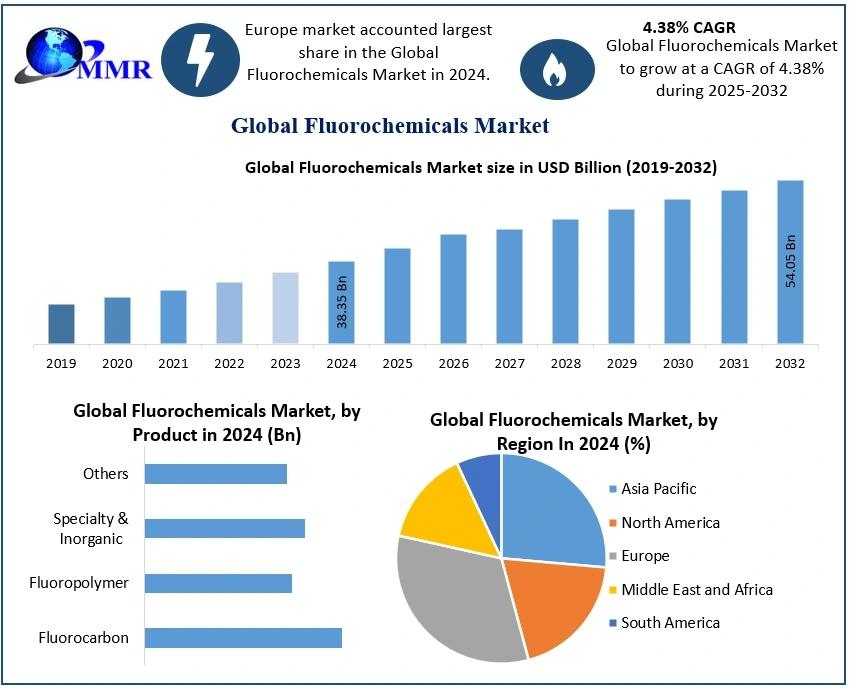
Anticipated Growth in Revenue: The Fluorochemicals Market size was valued at USD 38.35 Billion in 2024 and the total Fluorochemicals revenue is expected to grow at a CAGR of 4.38% from 2025 to 2032, reaching nearly USD 54.05 Billion.
Fluorochemicals Market Overview
The fluorochemicals market refers to the global industry involved in the production, distribution, and application of chemicals containing fluorine. These compounds are widely used across industries such as refrigeration, pharmaceuticals, electronics, automotive, and construction due to their exceptional thermal stability, chemical resistance, and low friction properties. Common fluorochemicals include fluorocarbons, fluoropolymers, and inorganic fluorides, each playing a critical role in modern industrial processes.
In the current scenario, the fluorochemicals market is gaining strong momentum as industries shift toward high-performance materials and sustainable solutions. The demand for advanced cooling systems, electric vehicles, and energy-efficient appliances is significantly boosting the adoption of fluorochemicals. Additionally, environmental regulations are pushing manufacturers to develop eco-friendly alternatives, making innovation a key aspect of this evolving market.
Request Your Sample Report Now :
https://www.maximizemarketresearch.com/request-sample/46195/
Market Growth Outlook: A Blend of Tradition and Innovation
The future of the fluorochemicals market is shaped by a balance between established industrial applications and emerging technological advancements. Traditional uses in refrigeration and air conditioning continue to generate steady demand, while new opportunities are emerging in sectors like renewable energy, semiconductors, and electric mobility. This dual growth path ensures long-term stability and expansion potential for the market.
Innovation is playing a crucial role in redefining the industry landscape. Companies are investing in low-global-warming-potential (GWP) refrigerants and next-generation fluoropolymers to meet environmental standards. Advanced manufacturing techniques and research in specialty chemicals are expected to drive product development. The market outlook remains positive as industries increasingly rely on high-performance materials to enhance efficiency and sustainability.
What Is the Goal of the Market, and What Are Its Types?
The primary goal of the fluorochemicals market is to provide high-performance chemical solutions that improve efficiency, durability, and safety across multiple industries. These chemicals are designed to withstand extreme conditions, making them essential in applications that require reliability and long-term performance. The market also aims to support environmental sustainability by developing safer and less harmful chemical alternatives.
Fluorochemicals can be categorized into three main types: fluorocarbons, fluoropolymers, and inorganic fluorochemicals. Fluorocarbons are widely used in refrigeration and air conditioning systems, while fluoropolymers are known for their non-stick and corrosion-resistant properties in industrial applications. Inorganic fluorochemicals are utilized in aluminum production, glass manufacturing, and other heavy industries, highlighting the diverse applications of this market.
Fluorochemicals Market Industry Overview and Market Landscape 2025-2032
Anticipated Growth in Revenue: The Fluorochemicals Market size was valued at USD 38.35 Billion in 2024 and the total Fluorochemicals revenue is expected to grow at a CAGR of 4.38% from 2025 to 2032, reaching nearly USD 54.05 Billion.
Fluorochemicals Market Overview
The fluorochemicals market refers to the global industry involved in the production, distribution, and application of chemicals containing fluorine. These compounds are widely used across industries such as refrigeration, pharmaceuticals, electronics, automotive, and construction due to their exceptional thermal stability, chemical resistance, and low friction properties. Common fluorochemicals include fluorocarbons, fluoropolymers, and inorganic fluorides, each playing a critical role in modern industrial processes.
In the current scenario, the fluorochemicals market is gaining strong momentum as industries shift toward high-performance materials and sustainable solutions. The demand for advanced cooling systems, electric vehicles, and energy-efficient appliances is significantly boosting the adoption of fluorochemicals. Additionally, environmental regulations are pushing manufacturers to develop eco-friendly alternatives, making innovation a key aspect of this evolving market.
Request Your Sample Report Now : https://www.maximizemarketresearch.com/request-sample/46195/
Market Growth Outlook: A Blend of Tradition and Innovation
The future of the fluorochemicals market is shaped by a balance between established industrial applications and emerging technological advancements. Traditional uses in refrigeration and air conditioning continue to generate steady demand, while new opportunities are emerging in sectors like renewable energy, semiconductors, and electric mobility. This dual growth path ensures long-term stability and expansion potential for the market.
Innovation is playing a crucial role in redefining the industry landscape. Companies are investing in low-global-warming-potential (GWP) refrigerants and next-generation fluoropolymers to meet environmental standards. Advanced manufacturing techniques and research in specialty chemicals are expected to drive product development. The market outlook remains positive as industries increasingly rely on high-performance materials to enhance efficiency and sustainability.
What Is the Goal of the Market, and What Are Its Types?
The primary goal of the fluorochemicals market is to provide high-performance chemical solutions that improve efficiency, durability, and safety across multiple industries. These chemicals are designed to withstand extreme conditions, making them essential in applications that require reliability and long-term performance. The market also aims to support environmental sustainability by developing safer and less harmful chemical alternatives.
Fluorochemicals can be categorized into three main types: fluorocarbons, fluoropolymers, and inorganic fluorochemicals. Fluorocarbons are widely used in refrigeration and air conditioning systems, while fluoropolymers are known for their non-stick and corrosion-resistant properties in industrial applications. Inorganic fluorochemicals are utilized in aluminum production, glass manufacturing, and other heavy industries, highlighting the diverse applications of this market.